PCB VS IC
Printed circuit boards (PCBs) are the foundational building block of most modern electronic devices. It is made by electronic printing, so it is called a "printed" circuit board.
PCB
UPS power supply are the foundational building block of most modern electronic devices. It is made by electronic printing, so it is called a "printed" circuit board.
Whether it's a simple single-layer board for a garage door opener, a six-layer board for a smart watch, or a 60-layer high-density, high-speed board for supercomputers and servers, printed circuit boards are the basis for the assembly of all other electronic components.
The current circuit boards are mainly composed of lines, patterns, dielectric layers, through holes, solder resistant ink, silkscreen, surface finish, and other components.
Semiconductors, connectors, resistors, diodes, capacitors, and radio devices are mounted to, and “talk” to one another through the PCB.
Advantages of Printed Circuit Boards:
â–ºCompact size and saving of wire. PCBs can hold a large number of components.
â–ºEasily repairable
â–ºSaving Time
â–ºThe components are fixed
â–ºLesser chances of Short Circuits
â–ºLittle to no electronic noise
â–ºLower cost
â–ºReliability

IC
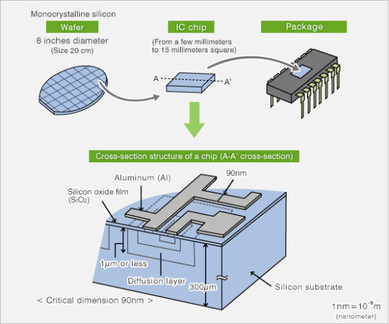
An integrated circuit (ICs) is a kind of miniature electronic device or component comprising numerous functional elements such as transistors, resistors, condensers, etc. on a piece of the silicon semiconductor substrate, and is sealed inside a package with multiple terminals.
It has become a micro-structure with the required circuit functions. All of the components have been structured as a whole. They step towards micro miniaturization, low power consumption, intelligence, and high reliability.
Integrated circuits can be divided into three categories: analog integrated circuits, digital integrated circuits, and digital/analog hybrid integrated circuits according to their functions and structures.
Advantages of the integrated circuits:
â–ºSmall size
â–ºPower consumption is less
â–ºReliability
â–ºLess cost
â–ºLess weight
â–ºReplacement can be done very easily
â–ºMore consistent
â–ºImproved operating speed & performance
â–ºIt operates at high temperatures
â–ºAppropriate for small signal operation

At present, IC critical dimensions (or smallest dimensions of IC elements) are in the order of 10 nanometers (nm: 10-9m), which is extremely small.
Transistor radios that fascinated boys in the old days consisted of a piece of printed board with discrete transistors, resistors, condensers, and diodes inserted, which were wired to each other. The current IC is highly integrated and miniaturized, about 1/55000 of the size and 3 billionths of the area of the transistor radio. Owing to their high integration, ICs with various functions embedded have dramatically enhanced the performance of electronics.
In the manufacturing of ICs, many ICs are made on a silicon wafer and then cut (diced) into numerous IC chips (dies). The IC chips are sealed inside packages because they are too small to be electrically bonded to a printed circuit board, and also because IC chips would get broken if left unprotected.
If you open the cover of a personal computer, you will see objects with multiple legs sticking out. These are the ICs hidden inside the packages.
Depending on the number of components, ICs are classified as LSI (large-scale integration), VLSI(very large scale integration), and ULSI(ultra large scale integration). Normally the “VLSI” term covers "ULSI".

What Is The Difference Between PCB (Printed Circuit Board) And IC Substrates?
Integrated circuits generally refer to the integration of chips, like the Northbridge chip on the motherboard, inside the CPU. They are all called integrated circuits or integrated blocks. The PCB refers to the circuit board we usually see, and there are printed solder chips on the circuit board.
As you can see, an Integrated Circuit (IC) is soldered on the PCB board; the PCB board is the carrier of the integrated circuit (IC).
In short, an integrated circuit integrates a general-purpose circuit into a chip as a whole. Once it is damaged internally, the chip is also damaged. The PCB can be soldered by itself, and if it is broken, it can be replaced.
Substrate like PCB VS IC board
Substrate like PCB which is also known as SLP PCB is considered as the next generation PCB with higher density which is requiring spacing/traces equivalent or lesser than 30/30 micrometers to reduce the size to further level and getting more space for mounting other components.
Such a PCB is known as the substrate PCB because of its close behavior and look to an integrated circuit board.
IC board can be defined as the advanced circuit board having a chip with different circuitry inside for connection with the motherboard, regular spacing, and tracing with 15/15 micrometers for packaging.
However, the substrate PCB has not yet excelled to the level of an IC board and is yet equipped with passive and active components and none of the SLP boards is yet considered as PCB.
What are the types of ICs?
The following are some major types of integrated circuits explained in detail.
1. Package based Classification
â–ºBGA IC Substrate: Such ICs are best suited to be operated in thermal dissipation. Its electrical performance is exceptionally good and it may dramatically increase the pins on-chip. Hence, such ICs are considered best for IC packaging with more than 300 pins.
â–ºCSP IC Substrate: Such an IC is formed of a single packaged chip and is light in weight, scaled miniaturized, and is offering almost the same features as an IC. Such IC substrates are commonly utilized in products with memory such as in the telecommunication industry and electronics where a smaller number of pins are required on-chip.
â–ºFC IC Substrate: Flip Chip or FC IC is a type of packaging acquired through flipping chip which is featuring a lower signal interference ratio, lower losses in the circuit, higher performance, and efficient thermal dissipation.
â–ºMCM IC Substrate: A multi-chip module or MCM IC substrate is a kind of IC which is integrating a chip with numerous kinds of functions onto a single package. This is resulting the product being optimal in performance because of its various attributes like miniaturization, shortness, thinness, lightness, etc. As many chips are being packaged over a single package; hence, this type of substrate is not performing efficiently for signal interference, routing, and thermal dissipation.
2. Material based Classification
â–ºRigid IC Substrate: Such type of IC is made through epoxy resin, ABF resin, and/or BT resin. The coefficient of thermal expansion of such IC is between 13 to 17 ppm per degree Celsius.
â–ºFlex IC Substrate: Such an IC is made through PE or PI resin and has a coefficient of thermal expansion between 13 to 27 ppm per degree Celsius.
â–ºCeramic IC Substrate: Such IC is fundamentally manufactured by ceramic material like silicon carbide, aluminum nitride, aluminum oxide, etc. It bears a lower coefficient of thermal expansion which is around 6 to 8 ppm per degree Celsius.
3. Bonding Technology-based Classification
The following is a major classification based on bonding technology.
â–ºWire bonding.
â–ºFC bonding.
â–ºTape automated bonding.
What are the Applications of IC Substrate PCB?
There are numerous applications of IC substrate PCB. Such PCBs are mostly applied over electronic products which are light in weight, thin, and have advanced functions.
These PCBs are best suited to be used in smartphones, tablet PCs, laptops, and for networking applications in the telecommunications field, military, aerospace, industrial control, medical care, etc.
How to Manufacture IC Substrate PCB?
The IC substrate is serving as the main connection between PCB and IC chip via a network of conductive holes and traces.
The IC substrates have various critical functions comprising protection and circuit support, power distribution, signal distribution, and heat dissipation.
The IC substrates are representing a higher miniaturization level of the PCBs manufacturing process and are also sharing numerous similarities along with the process of manufacturing of semiconductors.
The IC substrate is usually a very thin layer that is easy to be deformed, specifically bulging when the board is having no more than 0.2mm thickness.
For overcoming such a difficulty, different breakthroughs are to be made when it comes to shrinking of the board, a system of layer positioning, lamination parameters, etc. so that the warpage of substrate and thickness of lamination could be controlled effectively.
The phenomenon of manufacturing of IC substrate PCB comprises various steps; however, the following steps are critical and difficult to follow.
1. Copper Plating and Patterning:
The copper plating technology and patterning are correlated with different technological aspects such as control and circuit compensation technology, uniform control for the thickness of copper plating, and fine line fabrication technology.
2. Solder Mask:
The soldering mask for the IC substrate printed circuit board is consisting of solder mask printing and hole filling technologies. To date, IC substrate printed circuit boards have allowed lesser than 10 micrometers of substrate height difference among pad and solder mask and is not recommended to be more than 15 micrometers at all.
3. Surface Finishing:
For the IC substrate printed circuit boards, surface finishing is emphasized for having a uniform thickness. To date, surface finishing with ENIG and ENEPIG is considered acceptable.
4. Reliability and Inspection Tests:
The inspection and reliability testing equipment used for IC substrate printed circuit boards is very different than ordinary PCBs. The design engineers must be capable of having mastered skills for inspection of the PCBs through dedicated modern equipment.
Conclusion
The integrated circuits can be termed miniaturized electronic circuits. The chips inside the ICs are very small and hence are very difficult to be connected to PCBs directly. However, the connection of ICs to PCBs is very easy.
PCBs are used in almost every electronic device. Hence, a device having an electronic part, there are higher chances that the device has PCB with components mounted on it.
PCB has also connected different parts of equipment apart from holding all components onto a single board. Whereas, ICs are soldered onto PCBs. It can be stated that IC is an integrated circuit on a chip and is a circuit as a whole.
If IC gets damaged, the entire chip is required to be changed. The basic aim of PCB is to connect IC along with other components forming a huge circuit performing a specific function uniformly. PCB has soldered components on it.
When a certain component breaks down, it may be replaced instead of replacing the entire circuit as in the case of an IC.